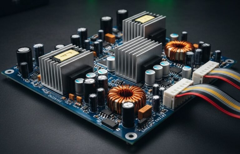
Solid-State Power Converters
We are advancing solid-state power converter technologies using wide-bandgap devices (SiC/GaN) for high efficiency, compact size, and intelligent control. Core areas include:
High-frequency switching for improved power density
Bidirectional converters for grid, storage, and EV systems
Intelligent digital control and real-time monitoring
Modular and scalable architectures
Enhanced protection and thermal management
These platforms enable next-generation solutions for smart grids, renewables, and electric mobility.
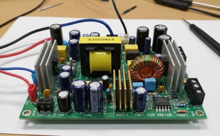
Advanced Power Converter Technologies
Our R&D spans a complete suite of high-performance power conversion systems:
DC–DC converters for regulated and isolated power delivery
AC–DC converters with stable, low-noise outputs
SMPS for compact, high-efficiency applications
Solar power converters optimized for maximum panel utilization
EV power modules supporting fast charging and high-power operation
Programmable laboratory power supplies built for precision R&D environments
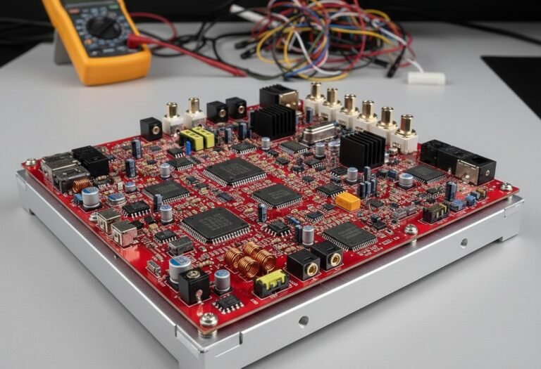
Customized Electronic Circuits
We specialize in designing and developing customized electronic circuits tailored for precision, performance, and application-specific requirements. Our R&D work focuses on three core areas:
Analog Circuit Design
Precision signal conditioning
Low-noise front-end circuits
Sensor interface modules
Filtering, modulation, and measurement circuits
High-stability reference and control circuits
Amplification Systems
Low-noise amplifiers (LNA)
High-gain instrumentation amplifiers
Power amplifiers for industrial and research applications
Wideband and high-frequency amplifier stages
Linear and switching amplifier architectures
Power Conversion Circuits
High-efficiency DC–DC and AC–DC stages
SMPS-based compact designs
Gate drivers and control circuits for power devices
Protection, monitoring, and feedback control circuitry
Custom power modules for EV, renewable, and industrial systems
Each solution is built to ensure reliability, thermal stability, noise immunity, and seamless integration into larger systems.
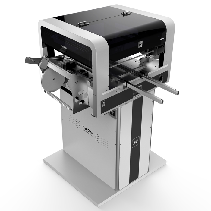
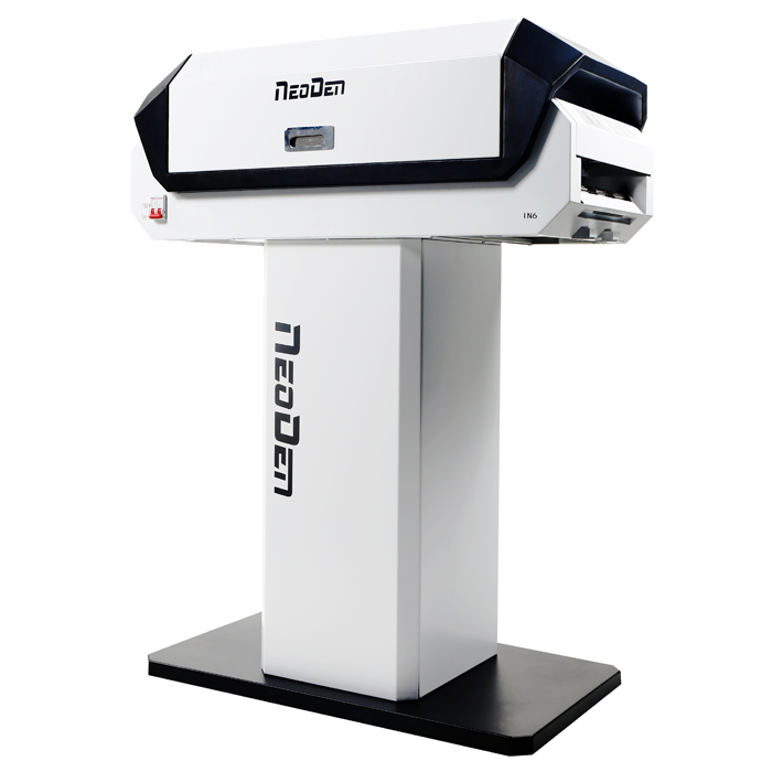
Advanced Automatic SMT Desktop Pick and Place machine
We maintain advanced R&D facilities in collaboration with KUMAR AUDIOS Company, enabling high-precision electronics development and prototyping. Our shared infrastructure includes the NeoDen N4+ Automatic SMT Desktop Pick-and-Place machine, equipped with a highly intelligent flying vision system—the first of its kind in its class. This fully automatic SMT platform enhances productivity through rapid, accurate component placement, achieving up to 5,000 CPH with the vision system and up to 10,000 CPH in the standard configuration. It supports a wide range of components from 0201 to TQFP240, including QFN, BGA, and SOT-23 packages, with flexible feeder options such as 48 tape reel feeders, vibrating tube feeders, and tray support. The system accommodates PCBs up to 310 × 1500 mm and integrates seamlessly with design tools like Altium, Eagle, and KiCad. Through this collaboration, we offer industry-grade electronic assembly capabilities for research, innovation, and product development.
Advanced Semi-Automatic SMT Reflow Oven
We have the NeoDen IN6 reflow oven as part of our R&D manufacturing setup, offering a compact and efficient solution for high-quality soldering. With precise temperature control, multiple heating zones, and a built-in smoke filtration system, it delivers consistent and reliable soldering performance for various PCB assemblies. Its user-friendly interface and versatile operation make it ideal for both rapid prototyping and medium-scale production, supporting clean, efficient, and modern electronic manufacturing workflows within our facility.
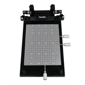
Manual SMT Solder Printer
We have a Manual Solder Printer for framed stencils, providing a simple and reliable method for applying solder paste to PCBs with consistent accuracy. This setup ensures clean, uniform deposition for both prototype and small-batch manufacturing, making the PCB assembly process efficient and repeatable in our R&D environment.
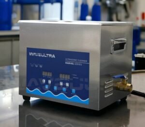
We have a digital-controlled ultrasonic cleaner for PCB cleaning, offering 500W of powerful ultrasonic action with multiple functions to ensure thorough and efficient removal of flux residues, dust, and contaminants. Its precise control system and high-frequency cleaning capability provide deep, uniform cleaning for delicate electronic assemblies, supporting reliable post-solder and maintenance workflows in our R&D facility.
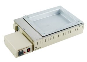
Digitally Controlled Lead Solder Pots
We have multiple-size, digitally controlled lead solder pots suitable for working on single PCBs from small to large, supporting board sizes up to 13x30 cm. These units provide stable temperature control and smooth solder flow, ensuring reliable tinning, desoldering, and manual assembly across a wide range of PCB sizes in our R&D workflow
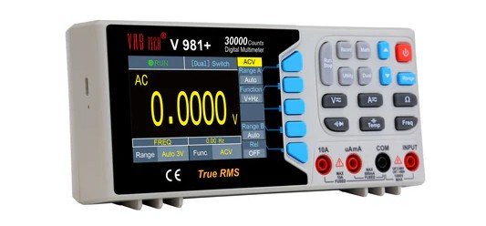
Advanced Metering and Measurement Tools
We have multiple measurement instruments, including dedicated meters for voltage, current, capacitance, inductance, and power, along with precision multimeters and customized meters capable of measuring a wide range of electrical and electronic parameters. Our facility is also equipped with oscilloscopes and signal generators for advanced waveform analysis and signal characterization. Together, these tools enable accurate testing, validation, troubleshooting, and detailed characterization across all our R&D activities.
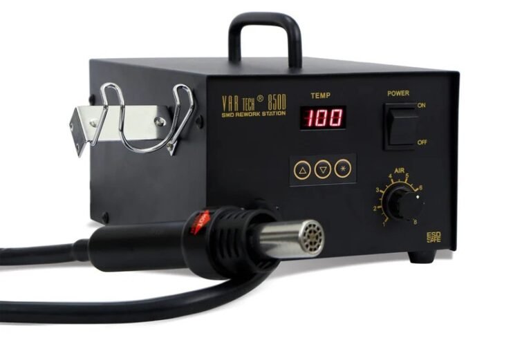
Precision SMD Assembly and Rework Tools
We have SMD rework stations and multiple SMD soldering stations, enabling precise component handling, removal, and soldering for a wide range of surface-mount devices. These tools support fine-pitch repairs, prototype assembly, and detailed rework operations across our R&D projects.